
A memory chip matters only when a factory can make it repeatedly. On September 20, Chinese manufacturer CXMT said its fifth-generation DRAM platform had reached mass production and that two 24-gigabit LPDDR5X products built on it were already being produced at scale. That is a company announcement, not an independent yield audit. But it marks a more consequential step than another laboratory sample: CXMT says a denser domestic process is now moving through a commercial line.
The numbers are specific. CXMT reports an active-area half-pitch of 11.95 nanometers, a memory-capacitor aspect ratio of 45:1 and at least 50% more 8-gigabit-equivalent dies per wafer than its previous platform. Reuters independently reported the announcement, while attributing the process measurements and production claims to the company.
The distinction matters. A small feature can demonstrate fabrication skill. Mass production asks whether thousands of process steps can deliver useful chips often enough, cheaply enough and reliably enough to ship.
DRAM is the computer’s working surface
Dynamic random-access memory, or DRAM, holds the data a processor needs immediately. It is different from flash storage: turn off the power and DRAM forgets. That volatility makes it fast enough to serve as a working surface for phones, computers and servers.
LPDDR5X is a low-power version designed for mobile devices. Each of CXMT’s new chips stores 24 gigabits, equal to 3 gigabytes before packaging and system configuration. CXMT says that is 50% more capacity than the comparable previous-generation product. More bits per die can let device makers offer more memory without simply adding more silicon area.
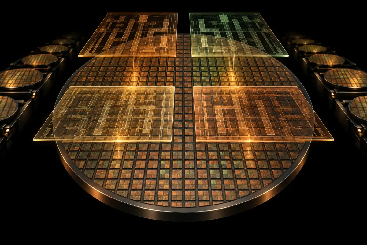
A chip factory prints many copies of tiny patterns onto a silicon wafer. Smaller memory cells can fit more useful chips on that wafer, but the printing becomes harder. CXMT says it now repeats one critical patterning sequence four times and is manufacturing the resulting chips at scale. The open question is how consistently the line produces good dies.
The “11.95 nanometer” figure needs careful reading. It is the reported half-pitch of the active area in the memory array: roughly half the repeating distance between neighboring features. It is not a universal process-node label, and it cannot by itself prove that the entire platform matches a rival’s technology.
Why four exposures can be worth the trouble
Optical lithography projects a pattern onto light-sensitive material on a wafer. As features shrink, one exposure can no longer define every line with enough separation. Multiple patterning splits one dense layout into several sparser masks. Each is printed and aligned in sequence, then combined into the final structure.
CXMT says G5 uses quadruple patterning for its memory array. The technique can extend existing lithography equipment to smaller spacing, but every additional exposure and alignment creates more opportunities for error. Overlay must be precise. A defect introduced in any pass can ruin a die. The interesting engineering claim is therefore not merely that four masks were used; it is that the company says the process is stable enough for volume manufacture.
DRAM also stores charge in extremely tall, narrow capacitors. CXMT’s reported 45:1 aspect ratio describes how deep those structures are relative to their width. That geometry is another reason density is difficult: shrinking the footprint does not remove the need to hold enough charge for the memory cell to be read reliably.
Density becomes economics at the wafer edge
A wafer has a fixed area. Smaller dies generally allow more copies to fit, although edge losses, redundancy and defect rates complicate the calculation. CXMT says its new process yields at least 50% more dies per wafer than G4 when both are normalized to an 8-gigabit product. That is a gross die-count comparison, not a disclosed percentage of saleable chips.
This is where manufacturing sovereignty becomes tangible. China’s chip strategy is often discussed through export controls and equipment access. But a domestic memory supplier becomes strategically useful only when its products can appear in real devices at predictable volume and cost. The new platform could widen the pool of suppliers for mobile memory. It does not establish that CXMT has matched Samsung, SK hynix or Micron in yield, endurance, power use or customer qualification.
CXMT also says it used a digital-twin system across design, development, manufacturing and maintenance. Simulated process models can reduce experiments and expose interactions earlier. They do not replace physical metrology or long production runs. A virtual line is useful precisely because the real one remains unforgiving.
The next evidence should arrive outside the announcement: product teardowns identifying the chips, customer qualifications, sustained shipment volumes and independent measurements of speed, power and reliability. Until then, the defensible conclusion is narrower but still important. CXMT is no longer presenting G5 only as a research capability. It is claiming that the process has crossed into repeatable manufacture—and inviting the market to test whether that claim holds.
Keep exploring
- These tiny devices remember by changing shape — a very different route to short-lived memory.
- Why Nvidia is pairing GPUs with a different kind of AI chip — how specialized hardware changes a computing pipeline.
- AI’s power problem is also a scheduling problem — why useful capacity is more than a peak benchmark.
AI-assisted. Sources checked.