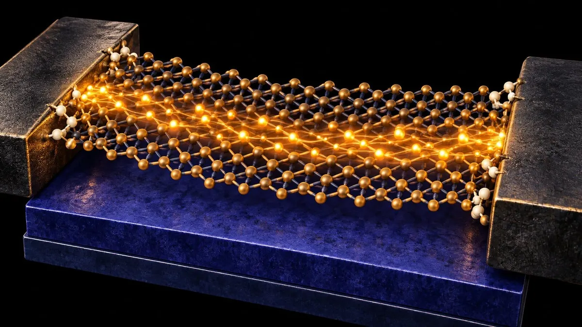
An atom-thin transistor carried 1,635 microamps of current per micrometer of channel width at room temperature. That is a striking number for the difficult p-type half of two-dimensional electronics. The device used a single layer of tungsten diselenide, or WSe2, treated with oxygen to repair defects and heavily dope the contact regions.
The accepted, peer-reviewed paper reports a 16-nanometer channel and contact resistance as low as 104 ohm-micrometers. Those measurements make the device a serious component experiment. They do not mean a complete processor has been built from one-atom-thick material, nor that the process is ready for mass manufacture.
In Plain English: Modern logic pairs two kinds of transistor. One switches using electrons; the other uses missing electrons, called holes. Pairing them lets a circuit avoid wasting power while it waits. Many atom-thin materials make stronger n-type devices than p-type ones. This study uses oxygen to help holes enter and cross a WSe2 transistor with much less resistance.
The Contact Can Waste the Channel's Advantage
The appeal of a two-dimensional semiconductor is physical thinness. An atomically thin channel gives a gate strong control over the flow of charge even when a device is extremely short. That could help transistor scaling beyond the point where conventional silicon channels become difficult to control.
But a channel is not useful if charge cannot enter it. Where metal meets a semiconductor, mismatched energy levels and metal-induced electronic states can create a barrier. In a p-type transistor, that barrier can leave useful “hole” current far below what the material itself should carry. The contact becomes a narrow, resistive doorway attached to a wide room.
The Nature Communications study attacks both the doorway and the room. Oxygen doping reduced selenium-vacancy defects in as-grown monolayer WSe2. The researchers report that hole mobility rose from 55 to 218.3 square centimeters per volt-second. Near the contacts, heavier oxygen doping increased the hole concentration and cut contact resistance from 1,869 to 104 ohm-micrometers.
That combination matters. Improving only the channel leaves the contact bottleneck. Improving only the contact still sends charge through a defective sheet. The reported device addresses both and reaches a saturation current density of 1,635 microamps per micrometer at a drain voltage of minus 1.2 volts.
Ballistic Does Not Mean Frictionless Manufacturing
The researchers describe the 16-nanometer device as ballistic because charge carriers cross most of the channel without scattering. They estimate a ballistic ratio as high as 81 percent at room temperature. In a very short channel, carriers have less distance in which defects and vibrations can redirect them, so current can approach a theoretical transport limit.
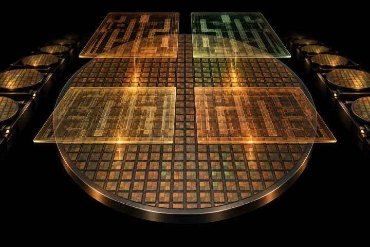
“Ballistic” does not mean the transistor has no resistance or consumes no energy. Contacts still resist current, the gate must control switching, and real circuits add interconnects, capacitance and heat. It also does not describe a production method. This experiment uses carefully grown monolayers and precisely fabricated test structures; a commercial chip would need billions of devices with narrow distributions, low leakage and durable contacts.
The paper is being shared as an accepted article before final copyediting. Its authors report no competing interests. The disclosed funding comes from Chinese national research programs and an industry-education integrated-circuit platform; those relationships explain support, not independent validation.
The Missing Proof Is a Complementary Circuit
The phrase complementary metal-oxide-semiconductor, or CMOS, refers to pairing n-type and p-type transistors so one network is normally off while the other is on. A strong p-type test device fills an important materials gap, but a complete logic family still needs matched thresholds, stable doping, low variability and manufacturing that places both polarities together.
The next useful demonstration would therefore be an inverter or larger circuit made from comparably scaled n- and p-type two-dimensional devices, tested for gain, switching energy, noise margin and endurance across a meaningful number of samples. Wafer-scale yield would matter more than another best-device record.
That distinction between a component and a system runs through Vastkind's coverage. MIT's soft nanodevices remember by changing shape, but still need a complete sensing task. CXMT says its new memory process has reached mass production, where yield becomes the test. And Nvidia's pairing of different AI chips shows why system performance depends on how specialized parts fit together.
Oxygen doping has made one p-type transistor substantially more convincing. The industry test begins when that strength survives repetition, integration and a whole circuit.
Production note: Vastkind reviewed the full public publication record and reported methods, performance and limitations. We did not fabricate or electrically test the devices.